In virtually every electronic device sold today, the conversion between different DC voltages now happens in a high-frequency switching power supply. These SMPS circuits can be tricky to design, so it's nice to be able to simulate them. Scroll through the screenshots below to learn how to build and simulate a boost converter (DC-DC step-up) in CircuitLab.
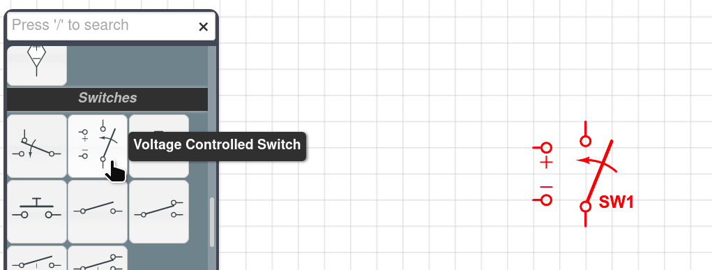
Scroll down in the toolbox to the Switches category. Click and drag a Voltage Controlled Switch onto your schematic:
Also drag on a Time Controlled Switch:

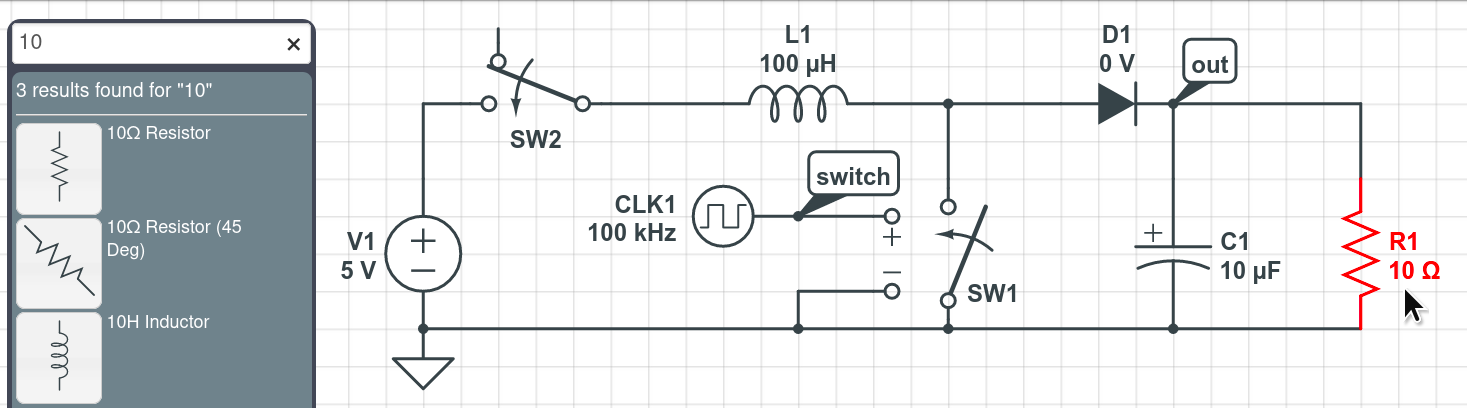
SW1 is the high-frequency switch of our power supply. (SW2 is used only to turn the circuit from off to on at t=0.)
While you're scrolling through the toolbox, click and drag to grab and insert a few more parts: a voltage source, a digital clock, an ideal diode, an inductor, and a capacitor, pressing R to rotate or H or V to flip:
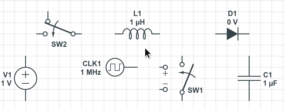
Click and drag from element endpoints to wire things up as shown:

(Make sure all four terminals of SW1 are connected.)
Let's set the values of all the components.
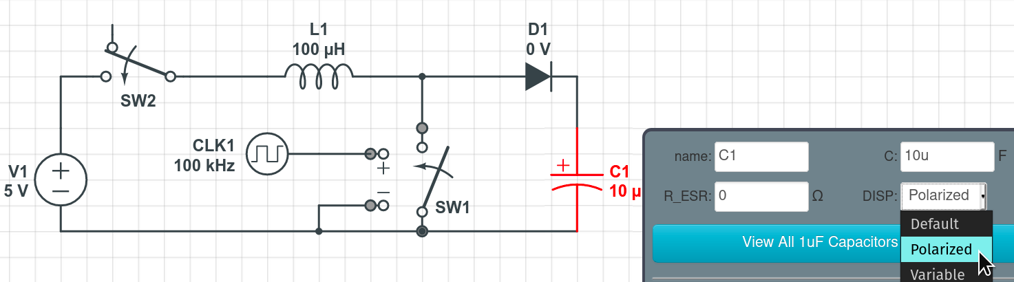
Double-click on V1 and set it to 5 volts. Double-click on L1 and make its inductance 100u. Double-click on CLK1 and set its frequency to 100k. Double-click on C1 and make it 10u, displaying as a Polarized capacitor:
Press G to add a ground node and click to place it at the bottom of V1:

Let's add node names so it's easier to see what's happening.
Press N and click to add a node name at the clock output, and do so again at the capacitor. Double-click to label these nodes "switch" and "out" respectively:
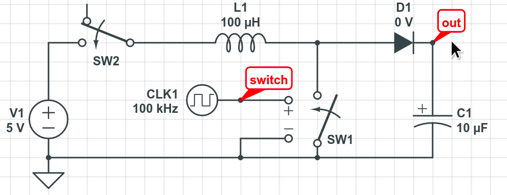
We've now finished building our basic boost converter. CLK1 turns SW1 on and off repeatedly, which first builds current in L1 while the switch is closed. When SW1 opens, the inductor maintains its current via D1, which charges C1.
Click Simulate at the bottom of the window, and click to expand the Time Domain tab:

Enter "1m" for Stop Time and "100n" for Time Step. Then, click on "out" and "switch" node name labels to add V(out) and V(switch) to the simulation Outputs list:

Click Run Time-Domain Simulation. A plot window appears:
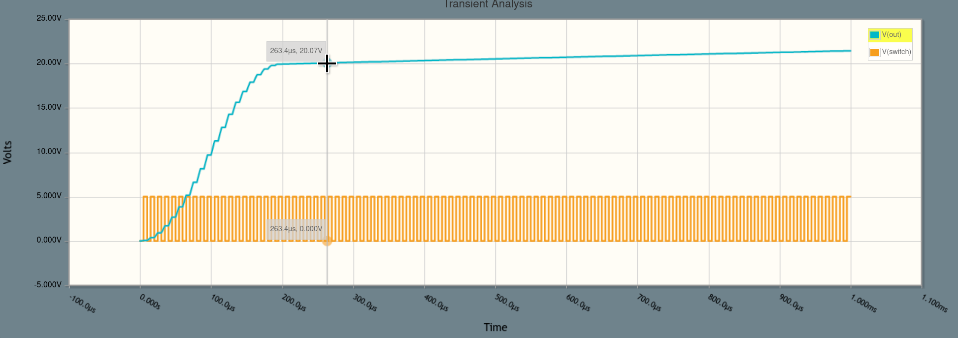
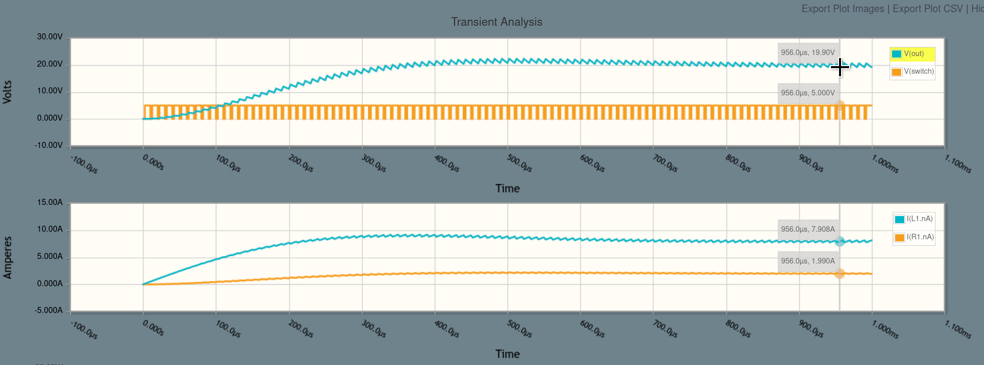
Our boost converter is working! With only a 5 volt input, it produces an output over 20 volts after a few cycles.
Let's add a load to our output.
Click Build at the bottom of the window to return to build mode. Press / (forward slash) to begin a toolbox search and type "10". Drag a 10 ohm resistor in parallel with C1, dragging to wire it up as shown:
Press F5 to repeat the simulation. A plot window appears:
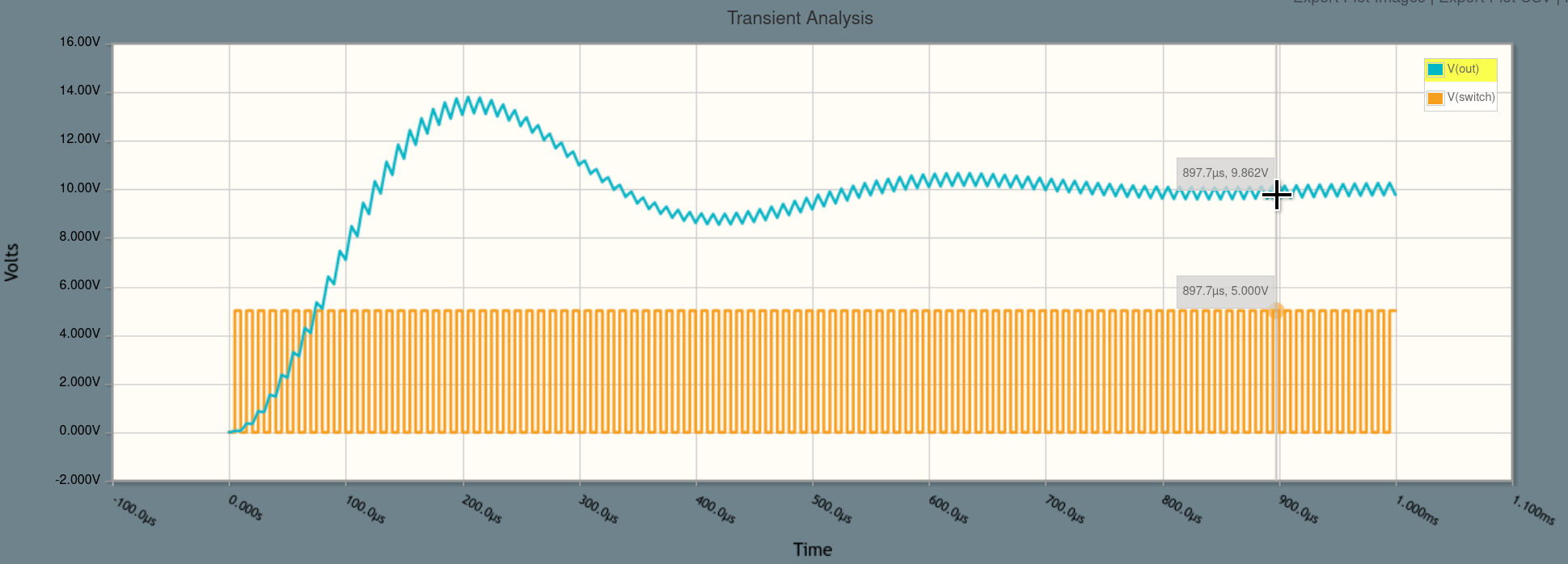
When loaded, the output voltage isn't quite as high, but it's still almost double our input voltage.
The triangular ripple in the output voltage is characteristic of switch-mode power supplies, and could be addressed by adding output filtering.
There's also overshoot and a bit of ringing before the voltage settles down. This can be fixed by adding a feedback control loop, rather than simply letting the clock run freely at 50% duty cycle.
Let's examine more of the circuit's behavior.
Click to focus the simulation settings window. Click + Add Expression and add four more expressions to the Outputs list: “I(L1.nA)”, “I(R1.nA)”, “-P(V1)”, and “P(R1)”

Click Run Time-Domain Simulation. A plot appears:

The top plot is in volts, and the second is in amps. We need to scroll down within the plot window to see the third plot with units of Watts:

The current plot shows us the instantaneous current through the load resistor R1 as well as through the inductor. Note that the steady-state current through the resistor is lower than that through the inductor, but it's at a higher voltage. So, as we can see in the 3rd chart of power consumption, the steady-state power flowing out of the voltage source V1 is approximately equal to the power flowing into the resistor R1.
This is only the case because we've made an ideal SMPS; we have no lossy components. We're using an ideal diode, an ideal switch, and we've modeled zero resistive losses in the inductor or capacitor. In reality, all of these components would be non-ideal, so the -P(V1) line would be above the P(R1) line, representing the efficiency of the design.
You can use CircuitLab to replace the ideal switch with a real n-channel MOSFET, for example, and replace the diode with a real PN junction diode, and you'll quickly see substantial losses. However, for early-stage design and education purposes, it's often best to start by working with ideal components, and only later incorporate nonidealities.
Let's try an experiment: what happens when we change the duty cycle of the clock signal driving the switch?
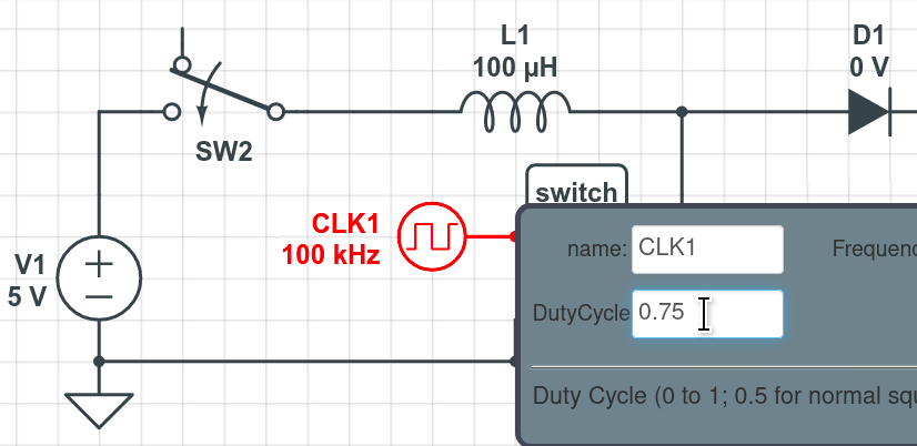
Click Build at the bottom of the window, and then double-click CLK1 and change its duty cycle from 0.5 to 0.75:
Press F5 to repeat the simulation. A plot window appears:
By raising the PWM duty cycle, we keep the switch closed longer, which allows more current to build up within the inductor each cycle. The result is a much higher output voltage -- about 20V, compared to 10V before -- and 4x the power delivered to the load.
If you're curious, you can remove CLK1 and replace it with a "PWM Generator" component, which turns an analog voltage into a PWM signal. By generating appropriate feedback from V(out), you can reduce overshoot and make the switching power supply hit a target output voltage for a wider range of loads.
That's it! You can now experiment with switch-mode power supplies in CircuitLab.
Click below to open the final circuit, or try it yourself from scratch (recommended).

CircuitLab is an in-browser schematic capture and circuit simulation software tool to help you rapidly design and analyze analog and digital electronics systems.