We’re introducing a new component to the CircuitLab toolbox: the ideal diode.
We’ve had semiconductor PN junction diodes since we’ve launched, which show the exponential current-voltage relationship and accurately model real-world diodes.
In contrast, the ideal diode is more like a simulated on-off switch: the I-V curve would be piecewise linear. It acts like it’s open-circuit when reverse biased, and short-circuit when forward biased. You can simply drag the ideal diode from the toolbox into your circuit, and optionally double-click to configure its parameters.
Here’s an example using four ideal diodes to build a full-wave rectifier:
Click to open and simulate the circuit above. Observe how the 4 diodes turn on and off at different times in the AC cycle.
Here’s an simulation comparing the regular PN Junction Diode with the ideal diode:
Click to open and simulate the circuit above.
Note that D2 (a PN junction diode) gives us a gentle knee as it transitions from off to on, as real diodes do. D2’s curve is smooth in the calculus sense: its derivative is continuous.
In contrast, ideal diodes D1 and D3 show an abrupt (piecewise-linear) knee when they change from off to on. These are not smooth in the calculus sense: their derivatives are discontinuous.
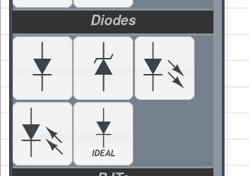
Both diode models, as well as Zener Diodes, photodiodes, and LEDs, are nows available in the CircuitLab toolbox:
In this tutorial video we build and simulate in an inverting amplifier with a chosen gain using an op-amp and other passive elements. We go over a few key concepts of an op-amps, introduce negative feedback, and build out a circuit that allows you to choose a specific gain for your inverting amplifier.
So I'm going to open up my CircuitLab editor here, and find the operational amplifier section, and I'm gonna drop this op amp onto my circuit. Op amps have lots of super cool properties, but I'm going to be using two big ones.
First, an op amp takes the difference of the two input voltages, and multiples that difference by a really really high number at the output voltage. This multiplication factor is the open loop gain of an op amp. We can see it here in the properties, it's the A_OL number, notice how all the device models have a different number, but the important thing is that number is a super high number, look em they're all in the hundreds of thousands or millions.
The other property is that no current (in reality very very little current) flows into or out of either of the input terminals. This will be important later.
The opamp models CircuitLab model the real devices based on the numbers in their datasheets. An "ideal" op amp which you may run into a problem set just has these properties maximally true, so the open loop gain is infinite and the input currents are actually 0.
Lets see these two properties in our simulation. [Show open loop gain in CircuitLab editor]
Ok so that's neat but not that useful because I want to be able to control this gain, just having an arbitrarily large number out here isn't helpful. So the first neat trick I'm going to use is negative feedback.
I'm gonna grab the output terminal and let's reason about what happens when I connect it directly to the minus input terminal. In this configuration, if something like a bit of noise in the universe was to make this voltage go up at the non inverting terminal, the output goes up, and the inverting input goes up, which makes the output go down. That output going down is fighting the original change.. And it balances out when there’s no difference between the two input terminals.
In this configuration, with negative feedback the op amp works to subtract any difference between the two input terminals. Meaning the inverting terminal will follow the non inverting terminal. We made a follower circuit!
So we are not there yet, let's introduce one more thing. I'm going to add a voltage source here, and two resistors. And I'm gonna call this one Rf, and this one Rin. Lets reason about this circuit. What is our output? We know in this configuration the difference between these two terminals is 0. The only way it can do that is by changing its output voltage and then measuring the two inputs again. We also know that no current can flow into or out of our input terminals. So I put a signal voltage here of 1, and if the op amp is forcing this to be 0, then our trusty friend V=IR says there is current flowing through this resistor, the other rule of the op amp says that current can't go into this terminal, so it has to go through this other resistor Rf. Again our trusty friend says if there is an IR there has to be voltage drop, and since it's the same I and R I think this voltage at out2 is going to be -1, and by golly it is.
So what if I make this Rf twice as large. Same input V, same Rin, so this current is the same, but now r is twice as much. Again V=IR so twice as much R and same I means twice as much Vout. Is it? Yes it is bloody exciting.
This means that just by changing the ratio of these resistors I can manipulate this circuit to have an arbitrary gain at its output!
You can find a link to this Circuit in the description of this video, you can open it up, change it and simulate it yourself to see what happens. If you found this helpful please like the video, and we will see you next time.
In this video tutorial we build and simulate a two input 2x1 digital mux using only NAND gates.
In this video we're going to build a two input multiplexer or two input digital mux made entirely out of NAND gates. So first what is a digital mux. A digital mux is a two input digital component that lets you select one of the two inputs based on the state of a third digital input.
CircuitLab has a digital mux component you can use, but that's not the point here, instead I'm going to be building my own entirely out of NAND gates.
So lets explore the NAND gate a little bit. Whenever I see a new component I like to simulate it just to see how it behaves. And the best way to do that is to just simulate it.
[Set up simulation with single NAND gate]
When the two inputs are digital low, the NAND gate makes the input high
Let's see what happens when I make one of these inputs a digital one. My V(out) is still high.
What happens when I make both inputs 1, now my V(out) is low. What I just went through is the truth table of a NAND gate.
[show truth table in CircuitLab]
That gives us a couple of very interesting properties. When one of the inputs is high, the output of a NAND gate is the opposite of the other input. I'm going to use that property later. Remember it.
The other property is that it's very easy to build an inverter using a NAND gate.
[set up NOT gate configuration]
So bear with me while I drop a whole bunch of gates into my circuit here.
[wire up the two input mux]
I'm going to name some nodes just to make it easier. This is my select node, and these two are going to be my input nodes. So what is going to happen in this configuration? What happens when I put a digital low at the select input. This puts a digital low at this NAND gate which means the output of this NAND gate is always high. Going back to the truth table, if any of the inputs are low the output is always high. So this in1 doesn't matter. The other thing this does, is because the output is always high then this nand gate is in that passthrough inverting configuration.
So lets go back to over here and see this NAND gate is a straight inverter here, which means this other NAND gate is also in this inverting pass through configuration. So in2 gets inverted twice, and ends up at the output.
And we can see if I switch this select node to be a 1, then the opposite happens: in2 doesn't matter and in1 gets inverted twice at the output! We made a digital mux!
CircuitLab is an in-browser schematic capture and circuit simulation software tool to help you rapidly design and analyze analog and digital electronics systems.